Impact of temperature on FIB irradiation induce damage: Ti and its alloys as examples of cryogenic focused ion beam milling of environmentally-sensitive materials
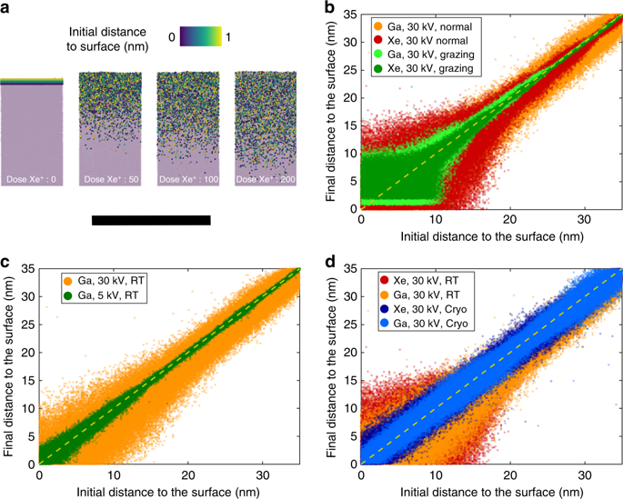
Hydrogen pick-up leading to hydride formation is often observed in commercially pure Ti (CP-Ti) and Ti-based alloys prepared for microscopic observation by conventional methods, such as electro-polishing and room temperature focused ion beam (FIB) milling. Here, we demonstrate that cryogenic FIB milling can effectively prevent undesired hydrogen pick-up. Specimens of CP-Ti and a Ti dual-phase alloy (Ti-6Al-2Sn-4Zr-6Mo, Ti6246, in wt.%) were prepared using a xenon-plasma FIB microscope equipped with a cryogenic stage reaching −135°C. Transmission electron microscopy (TEM), selected area electron diffraction, and scanning TEM indicated no hydride formation in cryo-milled CP-Ti lamellae. Atom probe tomography further demonstrated that cryo-FIB significantly reduces hydrogen levels within the Ti6246 matrix compared with conventional methods. Supported by molecular dynamics simulations (See Fig. 1), we show that significantly lowering the thermal activation for H diffusion inhibits undesired environmental hydrogen pick-up during preparation and prevents pre-charged hydrogen from diffusing out of the sample, allowing for hydrogen embrittlement mechanisms of Ti-based alloys to be investigated at the nanoscale. [See Chang et al. Nature Communications, 2019]

Fig. 1: Molecular dynamics (MD) simulations. a MD snapshots at different stages of the irradiation process of Xe at 30 kV in (0001)-oriented pure Ti surface at normal incidence. Atoms initially within 1 nm of the surface are indicated by the colour scale. The bulk atoms are shown in light purple. The scale bar is 10 nm. b Position of Ti atoms after irradiation (final distance to surface) as a function of their position before irradiation (initial distance to surface). c Similar graph as in (b) following Ga implantation at acceleration voltages of 5 kV (pink) and 30 kV (blue). d Similar graph as in (b) following Xe and Ga implantation at room temperature (RT) (dark red and orange respectively) and at cryogenic temperature, i.e., 138 K (light and dark blue respectively) [From Chang et al. Nature Communications, 2019]
Focused ion beam machining of strained silicon
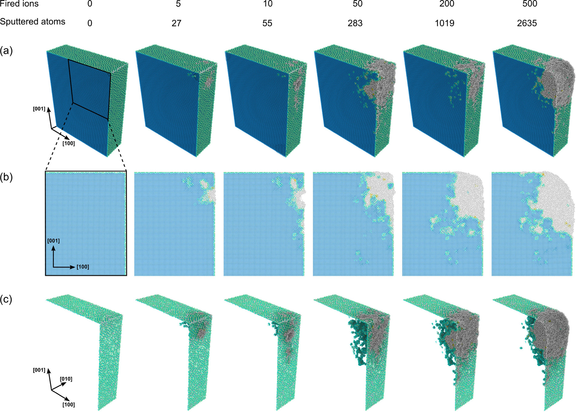
The focused ion beam (FIB) technique has established itself as an indispensable tool in the material science community, both to analyze samples and to prepare specimens by FIB milling. In combination with digital image correlation (DIC), FIB milling can, furthermore, be used to evaluate intrinsic stresses by monitoring the strain release during milling. The irradiation damage introduced by such milling, however, results in a change in the stress/strain state and elastic properties of the material; changes in the strain state in turn affect the bonding strength, and are hence expected to implicitly influence irradiation damage formation and sputtering. To elucidate this complex interplay between strain, irradiation damage and sputtering, we perform TRIM calculations and molecular dynamics simulations on silicon irradiated by Ga + ions, with slab and trench-like geometries, whilst simultaneously applying uniaxial tensile and compressive strains up to 4% (Fig. 2). In addition we calculate the threshold displacement energy (TDE) and the surface binding energy (SBE) for various strain states. The sputter rate and amount of damage produced in the MD simulations show a clear influence of the strain state. The SBE shows no significant dependence on strain, but is strongly affected by surface reconstructions. The TDE shows a clear strain-dependence, which, however, cannot explain the influence of strain on the extent of the induced irradiation damage or the sputter rate. [See Guenole et al. Applied Surface Science, 2017]

Fig. 2: Induced damage in collision cascade simulations of 5 kV Ga + ions in Si at 300 K. (a) Perspective view and (b) projected view of a slice with a thickness of 4 nm located at the simulation box center, i.e., with the highest concentration of incoming ions. (c) Perspective view where atoms in a perfect diamond cubic structure environment (until the second neighbor) are removed to highlight the irradiation-induced damage. toms are colored according the diamond structure identification method implemented in Ovito: blue – diamond cubic, cyan – diamond cubic structure with 1st and or 2nd neighbor in non-diamond structure environment, e.g. surfaces, white – non-diamond structure. [From Guenole et al. Applied Surface Science, 2017]
Influence of intrinsic strain on irradiation induced damage: the role of threshold displacement and surface binding energies
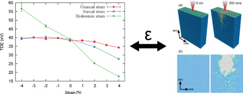
Current models for the formation of irradiation damage and the sputter yield are based on two key parameters, the threshold displacement energy (TDE) and surface binding energy (SBE), which are usually determined from unstrained systems with idealized surfaces. Here we use atomistic simulations to determine the TDE and SBE for strained silicon and aluminum and compare the results to full cascade simulations. A clear, material class dependent influence of the strain state on the TDE is observed, and surface amorphisation is shown to significantly increase the SBE of {001} surfaces. [See Guenole et al., Materials and Design, 2016]

Fig. 3: Average threshold displacement energy as function of applied strain mode, for Si. Applied strain modes considered are uniaxial ([010], red), equibiaxial (along [010] and [100] blue) and hydrostatic (green). Error bars correspond to the standard error of the data set (1000 independent values each). Solid lines are guides to the eye.
Induced damage in collision cascade simulations of 5 keV Ga + ions in Si at 300 K. Perspective view and projected view of a slice with a thickness of 4 nm located at the simulation box center, i.e. the highest concentration of incoming ions. [From Guenole et al., Materials and Design, 2016]
